Is it possible to Configure BLSP as SPI on DragonBoard820c?

QUP_MX_INPUT_CNT and OUTPUT are registers, 0x0200 and 0x0100 are their addresses not their values. They contain the number of word to read and write, and according to apq8016 technical manual (which has similar spi controller), the chip select is supposed to be asserted for a period derived from these values. So it would worth to write the values according to the expected word counts.

Also I notice that DMA mode is not enabled on MSM8996 (no dma channel associated), which can also be the cause of this limitation (FIFO mode is used).

Sorry, I meant the same :
512 words to read & 256 words to write

I also tried with : QUP_MX_OUTPUT_CNT = 0x0010
to write 16 words of 8 bits, the results observed were at 1Mhz:

As frequency of operation increases the performance is much degraded.

Any further insights on how to add support for this ??

Thanks in advanceā€¦

I donā€™t really know what happens, maybe itā€™s just a limitation of what can be achieved in FIFO mode, which is anyway used for small transfers. So it would require deeper investigation. One last thing to try would be maybe to replace any usleep_range() with udelay() in the driver in order to prevent context switching for SPI QUP state change.

Sure @Loic, will try to debug and update if any.

Hi @ljking

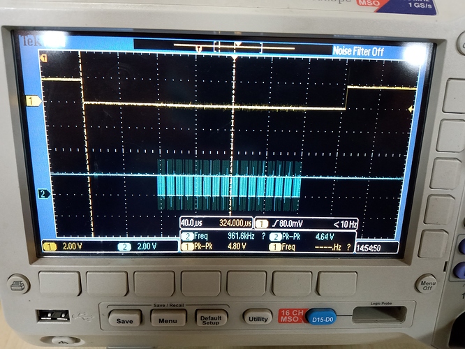
Is there any reason why CS is driven low one clock before & after ?

Thanks ,
Yash

Hi @ymj

Like almost any other interface, the chip select must be active before the data starts to arrive. If the chip select was to go active slightly after the data (say by 1ns), then the device receiving the information would have no idea that the information is intended for that device. if the chip select was to go active at exactly the same time as the data, then the receiving device might still miss it, due to delays in the wiring or in the transmitting and receiving circuitry.

In order to ensure that the receiving device knows that information is intended for that device the chip select must go active well in advance of the data. In this case (and with every SPI chip I have ever used) ā€œwell in advanceā€ is one clock time.

Same problem at the end of the data, if the chip select goes inactive too soon the receiving device might miss the data.

Here is a fragment from a typical SPI device datasheet.

As you can see the chip select must go active tcssc = 100nS before the the clock. The clock period tsclk is 250ns, this means that the chip select must go active about 1/2 clock time before the data, and every controller rounds this up to a full clock cycle. Same thing with tsccs at the end of the cycle.

Without the one clock before and after the data the SPI bus wouldnā€™t work.

@ljking thanks for the detailing on how to stop data loss.

Can you suggest ways to check if H/W CS is enabled and how it runs in accordance with CLK:

If it looks like this https://discuss-96boards-org.s3.amazonaws.com/original/1X/e07d0b61c5d53d27bda0746c9166db341de059c1.jpg then you have HW chip select. If it looks like your scope trace above you have user SW or driver SW chip select.